|
|
 发表于 2009-9-30 22:08:28
|
显示全部楼层
发表于 2009-9-30 22:08:28
|
显示全部楼层
nVidia GT300's Fermi architecture unveiled: 512 cores, up to 6GB GDDR5 9/30/2009 by: Theo Valich - Get more from this author
Just like we disclosed in the first article "nVidia GT300 specifications revealed – it's a cGPU!", nVidia GT300 chip is a computational beast like you have never seen before. In fact, we would go as far out and state that this is as closest as GPU can be to a CPU in the whole history of graphics technology. Now, time will tell whatever GT300 was the much needed revolution.
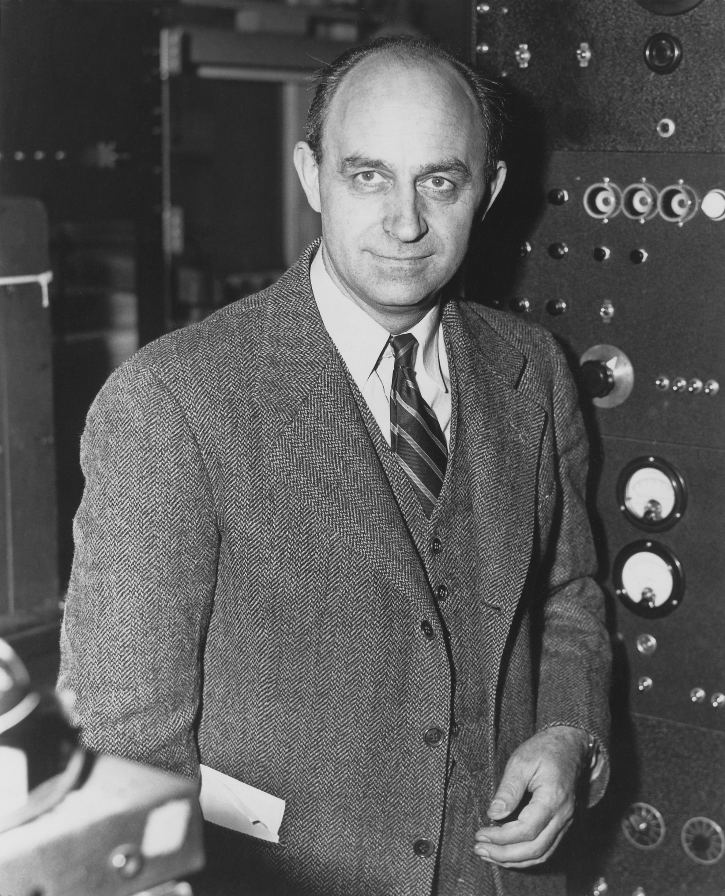
Beside the regular NV70 and GT300 codenames [codename for the GPU], nVidia's insiders called the GPU architecture - Fermi. Enrico Fermi was an Italian physicist who is credited with the invention of nuclear reactor. That brings us to one of codenames we heard for one of the GT300 board itself - "reactor".
When it comes to boards themselves, you can expect to see configurations with 1.5, 3.0 GB and 6GB of GDDR5 memory, but more on that a little bit later.
GPU specifications
This is the meat part you always want to read fist. So, here it how it goes:
3.0 billion transistors
40nm TSMC
384-bit memory interface
512 shader cores [renamed into CUDA Cores]
32 CUDA cores per Shader Cluster
1MB L1 cache memory [divided into 16KB Cache - Shared Memory]
768KB L2 unified cache memory
Up to 6GB GDDR5 memory
Half Speed IEEE 754 Double Precision
As you can read for yourself, the GT300 packs three billion transistors of silicon real estate, packing 16 Streaming Multiprocessor [new name for former Shader Cluster] in a single chip. Each of these sixteen multiprocessors packs 32 cores and this part is very important - we already disclosed future plans in terms to this cluster in terms of future applications. What makes a single unit important is the fact that it can execute an integer or a floating point instruction per clock per thread.
TSMC was in charge of manufacturing the three billion transistor mammoth, but it didn't stop there. Just like the G80 chip, nVidia GT300 packs six 64-bit memory controllers for a grand total of 384-bit, bringing back the odd memory capacity numbers. The memory controller is a GDDR5 native controller, which means it can take advantage of built-in ECC features inside the GDDR5 SDRAM memory and more importantly, GT300 can drive GDDR5 memory in the same manner as AMD can with its really good Radeon HD 5800 series. The additional two memory interfaces will have to wait until 28nm or 22nm full node shrinks, if we get to them with an essentially unchanged architecture. You can expect that the lower-end variants of GT300 architecture will pack less dense memory controller for more cost efficiency, especially on the memory side.
GPGPU is dead, cGPU lives!
Just like we reported earlier, GT300 changed the way how the GPU is functioning. If we compare it to the old GT200 architecture, comparisons are breathtaking. Fermi architecture operates at 512 Fused Multiply-Add [FMA] operations per clock in single precision mode, or 256 FMA per clock if you're doing double precision.
The interesting bit is the type of IEEE formats. In the past, nVidia supported IEEE 754-1985 floating point arithmetic, but with GT300, nVidia now supports the latest IEEE 754-2008 floating-point standard. Just like expected, GT300 chips will do all industry standards - allegedly with no tricks.
A GPU supports C++ natively?
Ferni architecture natively supports C [CUDA], C++, DirectCompute, DirectX 11, Fortran, OpenCL, OpenGL 3.1 and OpenGL 3.2. Now, you've read that correctly - Ferni comes with a support for native execution of C++. For the first time in history, a GPU can run C++ code with no major issues or performance penalties and when you add Fortran or C to that, it is easy to see that GPGPU-wise, nVidia did a huge job.
To implement ISA inside the GPU took a lot of bravery, and with GT200 project over and done with, the time came right to launch a chip that would be as flexible as developers wanted, yet affordable.
In a nutshell, this is just baseline information about what nVidia is going to introduce in the next couple of weeks. Without any doubt, we can see that nVidia reacted to Larrabee by introducing a part that is extremely efficient, natively support key industry standards and more importantly, doesn't cost an arm and a leg.
The line-up is consisted out of high-end consumer part [GeForce], commercial [Quadro] and scientific [Tesla]. You can expect memory sizes from 1.5GB for consumer GeForce 380 to 6GB for commercial Quadro and Tesla parts. |
|


 发表于 2009-9-29 15:24:03